eChook Nano – and the disappointing PCB manufacturing
Disappointingly we are having some issues with some of the boards from our first stack of eChook Nano v1.1’s. So far the quality of boards (v1 and other projects I have worked on) from dirtypcbs.com has been great, their cheap and fast service always delivering good quality boards without issue for my needs.
I was initially a little displeased when I received this latest batch, 12 eChook Nano boards, the first kit board we would send out for schools to test. I had hoped the schools would mostly be testing our documentation not our board quality!
The registration of the silk screen is quite poor. This means that the silk (black lettering/numbering) was not nicely centred on around the components. While this is annoying and leads to a less professional looking product I didn’t think of this as a major concern as it would not impact functionality and the board that was put together showed no signs of any issues and passed all of our tests.
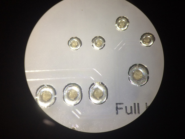
Looking in more detail at some of the other boards received (work have recently purchased a microscope for my lab) I noticed that it wasn’t just the silkscreen that wasn’t on centre. The pictures below show the extent of the problem quite well, with the plated pad area (shiny metal) clearly not centred in the area where the solder resist should be removed (the black area). The solder resist on these boards is the white stuff on top, this resists solder and makes a PCB much easier to solder together as it will stop the solder flowing, in our case down the tracks and potentially in to other components. Specifically here, because the board has a large ground plane pour, it will prevent a solder bridge of the PCB pad to the ground plane as the ground plane is hidden below this protective white layer of resist. This is important as (for all track apart from the ground pads), a short to ground will result in either incorrect readings of the sensor data, or worse, a damaged PCB.
Unfortunately…this hasn’t happened in this case. You can see in this lower image the tip of my multimeter probe, just skirting the edge of the solder resist. In this case I am checking around the 12V battery pin. Around the very edge of the white region I was finding my multimeter continuity test was showing this region as connected to ground, not good. This means that the ground plane is slightly showing through the solder resist. If I were to solder this pin it is likely that this would be bridged and cause a short between the 12V input and ground.
Can this all be blamed on the manufacturer of the PCB? Simple answer, no! Although the offset here has resulted in an issue I (as the PCB designer) could have taken steps to reduce the likelihood of this occurring. What I now realised I should have done is reduce the size of the area that is removed for the solder mask, effectively making the solder mask (white stuff) bigger and closer to the plated pad (a smaller black area). Doing this without changing the clearance of the pad area to the ground plan, this would have the effect of covering up a larger amount of the ground plane so even when the registration is poor between these parts of the PCB it is less likely to leave exposed ground plane showing.
An annoying blog post to have to write but a valuable lesson either way and certainly something that has added to my learning of the finer details of PCB design. The team will be modifying the gerbers and getting some new boards in to rectify this issue as soon as possible so we can get the kits out there!


Leave a Reply